- 您现在的位置:买卖IC网 > Sheet目录509 > SI4355-B1A-FM (Silicon Laboratories Inc)IC EZRADIO FM RECEIVER SI4355
�� �
�
�Si4355�
�5.2.1.� Shutdown� State�
�The� shutdown� state� is� the� lowest� current� consumption� state� of� the� device� and� is� entered� by� driving� SDN� (Pin� 2)�
�high.� In� this� state,� all� register� contents� are� lost� and� there� is� no� SPI� access.� To� exit� this� mode,� drive� SDN� low.� The�
�device� will� then� initiate� a� power� on� reset� (POR)� along� with� internal� calibrations.� Once� this� POR� period� is� complete,�
�the� POWER_UP� command� is� required� to� initialize� the� radio� and� the� configuration� can� then� be� loaded� into� the�
�device.� The� SDN� pin� must� be� held� high� for� at� least� 10� μs� before� driving� it� low� again� to� insure� the� POR� can� be�
�executed� correctly.� The� shutdown� state� can� be� used� to� fully� reset� the� part.�
�5.2.2.� Standby� State�
�The� standby� state� has� similar� current� consumption� to� the� shutdown� state� but� retains� all� register� values,� allowing� for�
�a� much� faster� response� time.� Because� of� these� benefits,� most� applications� will� want� to� use� standby� mode� rather�
�than� shutdown.� The� standby� state� is� entered� by� using� the� CHANGE_STATE� API� command.� While� in� this� state,� the�
�SPI� is� accessible� but� any� SPI� event� will� automatically� transition� the� chip� to� the� SPI� active� state.� After� the� SPI� event,�
�the� host� will� need� to� re-command� the� device� to� standby� mode.�
�5.2.3.� SPI� Active� State�
�The� SPI� active� state� enables� the� device� to� process� any� SPI� events,� such� as� API� commands.� In� this� state,� the� SPI�
�and� boot� up� oscillator� are� enabled.� The� SPI� active� state� is� entered� by� using� the� CHANGE_STATE� command� or�
�automatically� through� an� SPI� event� while� in� standby� mode.� If� the� SPI� active� state� was� entered� automatically� from�
�standby� mode,� a� CHANGE_STATE� command� will� be� needed� to� return� the� device� to� standby� mode.�
�5.2.4.� Ready� State�
�Ready� state� is� designed� to� give� a� fast� transition� time� to� RX� state� with� minimized� current� consumption.� In� this� mode�
�the� crystal� oscillator� remains� enabled� to� minimize� the� transition� time.� Ready� state� can� be� entered� using� the�
�CHANGE_STATE� command.�
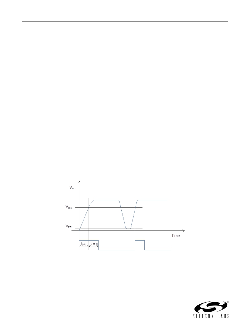
�5.2.5.� Power� On� Reset�
�A� Power� On� Reset� (POR)� sequence� is� used� to� boot� the� device� up� from� a� fully� off� or� shutdown� state.� To� execute� this�
�process,� VDD� must� ramp� within� 1ms� and� must� remain� applied� to� the� device� for� at� least� 10ms.� If� VDD� is� removed,�
�then� it� must� stay� below� 0.15V� for� at� least� 10ms� before� being� applied� again.� Please� see� Figure� x� and� Table� x� for�
�details.�
�Figure� 11.� POR� Timing� Diagram�
�22�
�Rev� 1.0�
�发布紧急采购,3分钟左右您将得到回复。
相关PDF资料
SI4388DY-T1-GE3
MOSFET DUAL N-CH 30V 8-SOIC
SI4390DY-T1-GE3
MOSFET N-CH 30V 8.5A 8SOIC
SI4396DY-T1-GE3
MOSFET N-CH D-S 30V 8-SOIC
SI4398DY-T1-GE3
MOSFET N-CH 20V 19A 8-SOIC
SI4404DY-T1-GE3
MOSFET N-CH D-S 30V 8-SOIC
SI4406DY-T1-GE3
MOSFET N-CH D-S 30V 8-SOIC
SI4410DY
MOSFET N-CH 30V 10A 8-SOIC
SI4411DY-T1-GE3
MOSFET P-CH D-S 30V 8-SOIC
相关代理商/技术参数
Si4355-B1A-FMR
功能描述:射频接收器 Si4355 EZRadio Rcvr
RoHS:否 制造商:Skyworks Solutions, Inc. 类型:GPS Receiver 封装 / 箱体:QFN-24 工作频率:4.092 MHz 工作电源电压:3.3 V 封装:Reel
SI4355-B1A-GM
制造商:Silicon Laboratories Inc 功能描述:SI4355 EZRADIO RECEIVER - Bulk
SI4356ADY
制造商:VAISH 制造商全称:VAISH 功能描述:N-Channel 30-V (D-S) MOSFET
Si4356ADY-T1-E3
功能描述:MOSFET 30V 26A 6.5W RoHS:否 制造商:STMicroelectronics 晶体管极性:N-Channel 汲极/源极击穿电压:650 V 闸/源击穿电压:25 V 漏极连续电流:130 A 电阻汲极/源极 RDS(导通):0.014 Ohms 配置:Single 最大工作温度: 安装风格:Through Hole 封装 / 箱体:Max247 封装:Tube
SI4356ADY-T1-GE3
功能描述:MOSFET 30V 26A 6.5W 5.5mohm @ 10V RoHS:否 制造商:STMicroelectronics 晶体管极性:N-Channel 汲极/源极击穿电压:650 V 闸/源击穿电压:25 V 漏极连续电流:130 A 电阻汲极/源极 RDS(导通):0.014 Ohms 配置:Single 最大工作温度: 安装风格:Through Hole 封装 / 箱体:Max247 封装:Tube
SI4356-B1A-FM
制造商:Silicon Laboratories Inc 功能描述:SI4356 STANDALONE SUB-GHZ RECE 制造商:Silicon Laboratories Inc 功能描述:SI4356 STANDALONE SUB-GHZ RECEIVER - Rail/Tube 制造商:Silicon Laboratories Inc 功能描述:IC RX SUB-GHZ STAND ALONE QFN 制造商:Silicon Laboratories Inc 功能描述:RF Receiver Si4356 Standalone Sub-GHz Receiver
SI4356-B1A-FMR
制造商:Silicon Laboratories Inc 功能描述:SI4356 STANDALONE SUB-GHZ RECE 制造商:Silicon Laboratories Inc 功能描述:RECEIVER RF CI SMD - Tape and Reel 制造商:Silicon Laboratories Inc 功能描述:RF Receiver Si4356 Standalone Sub-GHz Receiver
SI4356DY
制造商:VISHAY 制造商全称:Vishay Siliconix 功能描述:N-Channel 30-V MOSFET